


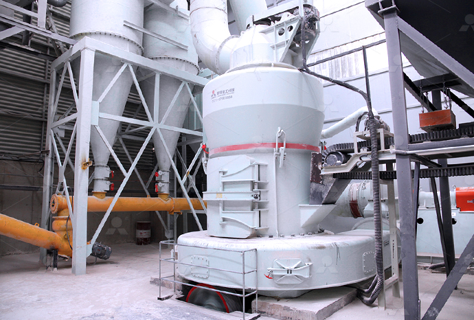
MTW European Type Trapezium Mill
Input size:30-50mm
Capacity: 3-50t/h
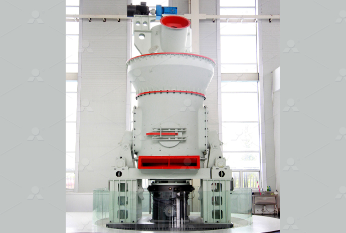
LM Vertical Roller Mill
Input size:38-65mm
Capacity: 13-70t/h
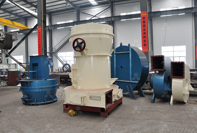
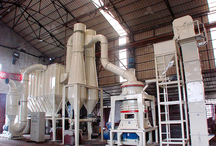
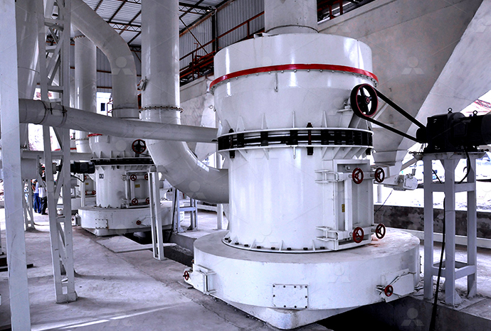
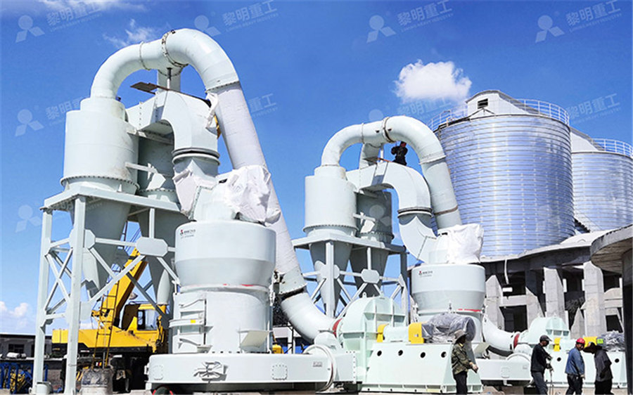
Raymond Mill
Input size:20-30mm
Capacity: 0.8-9.5t/h
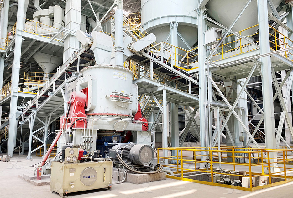
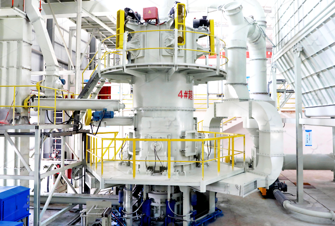
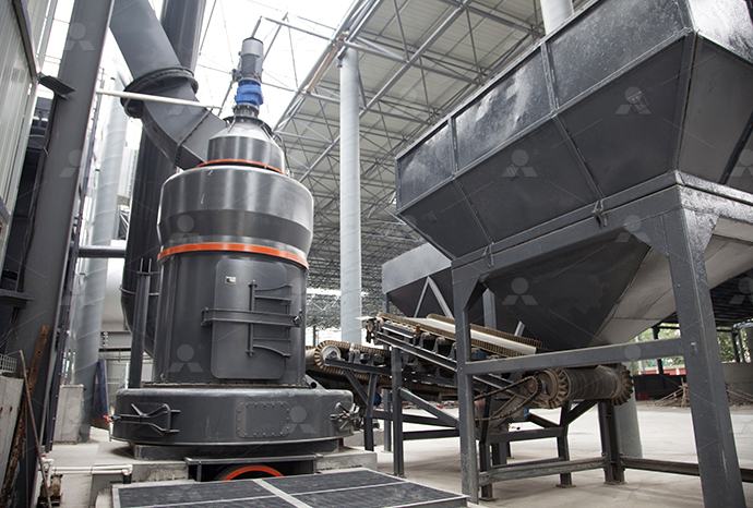
Sand powder vertical mill
Input size:30-55mm
Capacity: 30-900t/h
LUM series superfine vertical roller grinding mill
Input size:10-20mm
Capacity: 5-18t/h
MW Micro Powder Mill
Input size:≤20mm
Capacity: 0.5-12t/h
LM Vertical Slag Mill
Input size:38-65mm
Capacity: 7-100t/h
LM Vertical Coal Mill
Input size:≤50mm
Capacity: 5-100t/h
TGM Trapezium Mill
Input size:25-40mm
Capacity: 3-36t/h
MB5X Pendulum Roller Grinding Mill
Input size:25-55mm
Capacity: 4-100t/h
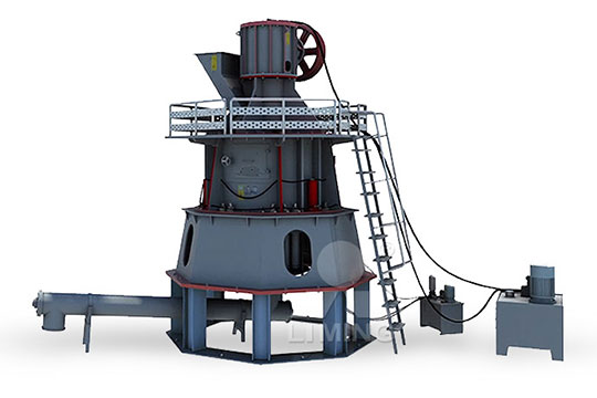
Straight-Through Centrifugal Mill
Input size:30-40mm
Capacity: 15-45t/h
Silicon micropowder deep processing
Crack Formation Reduction on DiamondPaste Abrasive
2023年10月2日 Sizes of Surface Microcracks in Silicon Carbide Wafers and Material Removal Rate with Varying Abrasive Treatment Regimes The use of ASM 40/28 diamond micropowder 2022年5月2日 A deep etching method of micropatterns on Si based on metalassisted chemical etching was successfully developed, which was impossible with the common MACE process In this deep MACE, the critical improvement was Deep Etching of Silicon Based on MetalAssisted Abstract:In this paper,the raw material characteristics,modification process,surface modification method and selection of modifier,modifier dosage,modification process conditions of siliconResearch progress of surface modification and application of Silicon Devices and Process Integration covers stateoftheart silicon devices, their characteristics, and their interactions with process parameters It serves as a comprehensive guide which addresses both the theoretical and practical Silicon Devices and Process Integration: Deep
.jpg)
Silicon Powder Properties Produced in a Planetary Ball Mill as a
2020年1月15日 In this study a metallurgical grade silicon quality was milled in a planetary ball mill and the properties of the powder were investigated as a function of grinding time, grinding 2019年12月27日 Microfluidic devices can be manufactured from a wide range of materials, such as transparent silicone elastomer (polydimethylsiloxane (PDMS)), thermoplastics (eg polymethylmethacrylateMaskless, rapid manufacturing of glass microfluidic 2021年8月17日 With the ultrafine processing of nonmetallic minerals, ultrafine crushing and grading technology has become one of the most important deep processing technologies, Ball mill and classifying production line of silica powder2020年5月12日 Herein, we demonstrate the relationship between the size of the scallop nanostructure and the profile of the deep silicon microstructure, which is beneficial for judging The application of the scallop nanostructure in deep silicon etching
.jpg)
High speed silicon wet anisotropic etching for
2021年2月22日 Wet anisotropic etching is extensively employed in silicon bulk micromachining to fabricate microstructures for various applications in the field of microelectromechanical systems (MEMS) In addition, it is most widely used 2023年9月1日 Silica micropowder (SMP) is a kind of quartz powder with high purity It is obtained by selecting, crushing, grinding [8], and acidpurifying processes of natural quartz [9, Formulation optimization and performance enhancement of 2016年11月1日 The resultant content of silicon carbide in Si/SiC ceramics and, correspondingly, its bulk density, is strongly affected by the processing conditions on every stage, starting from the preparation of raw materials Powder injection molding (PIM) is a well known and efficient method for fabrication of ceramic articles [19]Powder injection molding of silicon carbide: processing issues2023年10月2日 The results of diamondabrasive processing of the backside of 4H and 6Hpolytype siliconcarbide semiconductor wafers are presented The sizes of surface microcracks in ceramic plates after abrasive treatment by means of pastes with diamond micropowder of various grain sizes were investigated, and the relationship between the length of a surface microcrack Crack Formation Reduction on DiamondPaste Abrasive Processing
Micropowder injection molding ScienceDirect
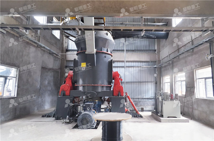
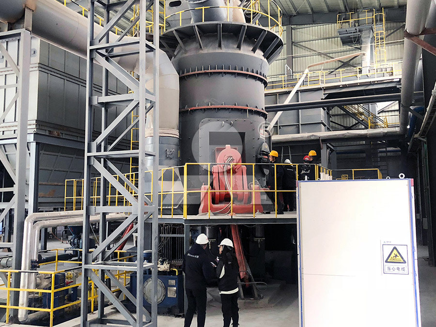
2002年9月30日 Fig 2 shows the silicon mold inserts with square or round cavities The silicon mold inserts were made by deep reactive ion etching Their dimensions are 100 μm ×100 μm, and φ100 μm, with a depth of 250 μm, giving an aspect ratio of 25 The cavities were “blind holes” Download : Download fullsize image Fig 22018年4月17日 The silicon wafer was initially etched through deepreactive ion etching (DRIE) step for an etch depth of 5 μm (Fig 2b); Then silicon oxide film 200 nm in thickness was formed on the surface of Key Processes of SiliconOnGlass MEMS Fabrication Technology 2021年6月15日 Silicon carbide (SiC) ceramics have become a significant specialty material for advanced applications such as gasturbine, nuclear power, semiconductor, and aerospace industries because of their high thermal conductivity and resistance thermal shock, corrosion resistance, chemical inertness, and abrasion resistance [[1], [2], [3]]Recent interest in Polymerderived silicon carbide micro powders through selective Fine grinding: Use a 600mesh silicon micropowder ultrafine grinder to grind to meet the qualified particle size requirements Classification: The finely ground silicon powder needs to be classified by air flow to ensure that the particle size distribution meets the requirements 600 mesh silicon powder ultrafine grinding machine introductionNews 600 mesh silicon micropowder ultrafine grinding machine
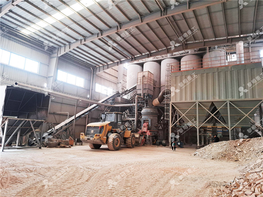
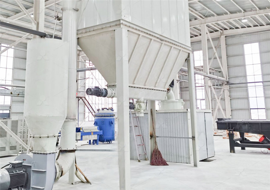
Grinding Mills, Ultrafine Mills, Powder Processing Equipment
Comparison of industrial silicon powder processing equipment As a manufacturer of industrial silicon powder processing equipment, Guilin Hongcheng has Raymond mill, vertical mill and ring roller mill to choose from The grinding process and grinding equipment determine the particle size and particle composition of silicon powder2022年10月7日 (a) Illustration of the micromachined silicon vapor cell The cell is composed of a borosilicate glass (BSG)SiBSG stack, with total outer dimensions of (13 mm) 2 Â 7 mmMicromachined deep silicon atomic vapor cells ResearchGate2019年8月26日 This paper presents the fabrication of silicon hollow microneedles by a deepreactive ion etching S J Handbook of Advanced Plasma Processing Techniques (SpringerVerlag, Berlin Heidelberg, Fabrication of sharp silicon hollow microneedles by deepreactive 5 Silicon carbide nanopowder is also used to produce aerospace mirrors The material was used because it is very rigid and resistant to thermal shock Silicon carbide also prevents mechanical fatigue, moisture absorption and deterioration caused by space radiation 6 Silicon carbide is well known as an effective material in armor protectionSilicon Carbide (SiC) Micron and Nano Powder Nanografi
Scanning Strategy Investigation for Direct Powder Bed
2022年1月13日 DirectPowder Bed Selective Laser Processing (DPBSLP) is considered a promising technique for the Additive Manufacturing (AM) of Silicon Carbide (SiC) For the successful DPBSLP of SiC, it is necessary to Wet Silicon BulkMicromachining This micromachining technique has been used for more than two decades and is the most popular fabrication technology for sensors such as pressure sensors and accelerometers []In this bulkmicromachining, chemical etching solutions are used to shape the microstructures by the removal of a large amount of single crystalline silicon substrateSilicon Micromachining SpringerLinkSilicon Processing Techniques Thomas Ortlepp, Tobias Wittig 9th Beam Telescopes and Test Beams Workshop ONLINE 08022021 3D processing necessary • making use of Deep Reactive Ion Etching (DRIE) to drill holes into the bulk • Silicon Processing Techniques2000年8月1日 In this paper, a backincidence 3D Composite Electrode Silicon Detector (3DCESD) is proposed and simulated The electrode structure comprises 70% trenchlike and 30% columnlike features, achieved Loading effects in deep silicon etching ResearchGate
.jpg)
Micro ED Milling of Ti6Al4V with SiC Nano Powder Mixed
Micro ED milling is one of the widely applied processes to generate microfeatures on electrically conductive materials However, the drawbacks associated with this process namely low MRR and high surface roughness limits its wide applicability To enhance the rate of metal removal and surface finish an investigation is carried out by mixing SiC nano powders with dielectric media 2022年4月15日 Request PDF Silicon microring synapses enable photonic deep learning beyond 9bit precision Deep neural networks (DNN) consist of layers of neurons interconnected by synaptic weights A high Silicon microring synapses enable photonic deep learning beyond 2020年3月23日 A novel 3D silicon shaping technology has been developed that combines a multistep etching process with corner lithography Currently, system miniaturization relies extensively on 3D machining Waferscale 3D shaping of high aspect ratio structures by High purity Silica, also known as Silicon dioxide, is one of the most subtle yet prominent materials in the world It is the main filler in a lot of products, including semiconductor molding compounds, optical fibers, coating powder but also in building materials, solar panels and high performance ceramics The list doesn't stop hereHigh Purity Silica Fine Specialty Chemicals Caplinq
High Purity Porous Silicon Powder Synthesis by Magnesiothermic
2021年3月1日 Here, the capacity of various nanocages (C70, Al35N35, Si52, B26N26, Ge60 and B30P30) as anodes in batteries is calculated Here, the novel materials (Al35N35, B26N26 and B30P30) with high Silicon powder improves the performance of your product Silicon powder, also known as micronized silicon, is used for many different applications Silicon powder improves the performance of your product Skip to main Different purities and sizes are therefore available, to satisfy customer processing requirements and application needsWhat is silicon powder? ElkemSilicon Deep Trenches with Extremely Vertical Smooth Sidewalls Used in MicroOptical Gyroscopes Micromachines 2023, 14, 846https:// etching [21–23] Femtosecond laser processing focuses a laser beam on the surface of a workpiece through an optical system, thereby melting and vaporizing the material to Micromachines 2023, 14, 846https: Inductively Coupled Plasma Dry Etching of Silicon Deep Trenches 2021年4月1日 The study was carried out to investigate the manufacturing possibility of Silicon Carbide (SiC) by direct Powder Bed Selective Laser Processing (PBSLP) experimentally and numericallyExperimental and numerical study for direct powder bed selective
Feasibility investigation on ductile machining of singlecrystal
2019年9月1日 In contrast, diamond cutting technologies, such as diamond milling, diamond sculpturing and fast and slow tool serve (FTS/STS), is more flexible in the ductile machining of brittle materials for freeform surfaces and microstructures [[17], [18], [19], [20]]By means of slow tool servo, 55 μm deep microlens arrays were machined on singlecrystal silicon by Mukaida 2020年5月4日 The demand for crystalline silicon wafers is continuing to increase It is inevitable that highpurity silicon will be lost as loose abrasive slurry silicon powder (LASSP) and diamond wire saw silicon powder (DWSSP) during the process of wafer preparation For this reason, some advanced processes or methods require further development to solve the problems of the high Review of Silicon Recovery and Purification from Saw Silicon Powder2023年11月23日 Silicon nanoparticles have emerged as pivotal components in nanoscience and nanoengineering due to their inherent characteristics such as high energy capacity and outstanding optical properties Numerous fabrication and characterization techniques have been researched so far, while a range of applications utilizing them have been developed In this Silicon nanoparticles: fabrication, characterization, application and A diagram of the semiconductor oxide transistors made by Frosch and Derick in 1957 [24] In 1955, Carl Frosch and Lincoln Derick, working at Bell Telephone Laboratories, accidentally grew a layer of silicon dioxide over the silicon wafer, for which they observed surface passivation effects [25] [26] By 1957 Frosch and Derick, using masking and predeposition, were able to Semiconductor device fabrication Wikipedia
Study of deep silicon etching for microgyroscope fabrication
2001年6月1日 Deep silicon etching for fabrication of the microgyroscope has been studied Effects of feature size, platen power and processing pressure on etching rate of silicon and photoresist are investigated Experimental results indicate that etching rate of silicon increases with increasing platen power, process pressure and feature size2022年4月13日 The effect is due to ion flux differences between low and high Aspect Ratio features and to the ability of etch processing in smaller openings []When the lower etch rate occurs in the larger feature, the effect is called inverse RIE Lag [] Table 51 summarizes the terminology related to the Bosch process, just to better understand the technical challenges Deep Silicon Etch SpringerLinkHere are some of the applications of silicon powder: Chemical Industry: Silicon powder is used as a raw material in the chemical industry for the production of various siliconbased compounds, such as silicones, silanes, and other organosilicon products These compounds have numerous applications in adhesives, sealants, lubricants, and coatingsSilicon MicroPowder Nanorh2012年1月1日 Laser radiation can be produced in different operating modes (continuous, pulsed) and in different media (solidstate lasers, gas lasers) Pulse durations range from microseconds to femtoseconds, as in pulsed excimer gas lasers which radiate in the deep UV (wave length 157–351 nm) and femtosecond or millisecond pulsed solidstate lasers Laser Micro and Nano Processing of Metals , Ceramics , and
.jpg)
Powder injection molding of silicon carbide: processing issues
2016年11月1日 The resultant content of silicon carbide in Si/SiC ceramics and, correspondingly, its bulk density, is strongly affected by the processing conditions on every stage, starting from the preparation of raw materials Powder injection molding (PIM) is a well known and efficient method for fabrication of ceramic articles [19]2023年10月2日 The results of diamondabrasive processing of the backside of 4H and 6Hpolytype siliconcarbide semiconductor wafers are presented The sizes of surface microcracks in ceramic plates after abrasive treatment by means of pastes with diamond micropowder of various grain sizes were investigated, and the relationship between the length of a surface microcrack Crack Formation Reduction on DiamondPaste Abrasive Processing 2002年9月30日 Fig 2 shows the silicon mold inserts with square or round cavities The silicon mold inserts were made by deep reactive ion etching Their dimensions are 100 μm ×100 μm, and φ100 μm, with a depth of 250 μm, giving an aspect ratio of 25 The cavities were “blind holes” Download : Download fullsize image Fig 2Micropowder injection molding ScienceDirect2018年4月17日 The silicon wafer was initially etched through deepreactive ion etching (DRIE) step for an etch depth of 5 μm (Fig 2b); Then silicon oxide film 200 nm in thickness was formed on the surface of Key Processes of SiliconOnGlass MEMS Fabrication Technology
.jpg)
Polymerderived silicon carbide micro powders through selective
2021年6月15日 Silicon carbide (SiC) ceramics have become a significant specialty material for advanced applications such as gasturbine, nuclear power, semiconductor, and aerospace industries because of their high thermal conductivity and resistance thermal shock, corrosion resistance, chemical inertness, and abrasion resistance [[1], [2], [3]]Recent interest in Fine grinding: Use a 600mesh silicon micropowder ultrafine grinder to grind to meet the qualified particle size requirements Classification: The finely ground silicon powder needs to be classified by air flow to ensure that the particle size distribution meets the requirements 600 mesh silicon powder ultrafine grinding machine introductionNews 600 mesh silicon micropowder ultrafine grinding machine Comparison of industrial silicon powder processing equipment As a manufacturer of industrial silicon powder processing equipment, Guilin Hongcheng has Raymond mill, vertical mill and ring roller mill to choose from The grinding process and grinding equipment determine the particle size and particle composition of silicon powderGrinding Mills, Ultrafine Mills, Powder Processing Equipment2022年10月7日 (a) Illustration of the micromachined silicon vapor cell The cell is composed of a borosilicate glass (BSG)SiBSG stack, with total outer dimensions of (13 mm) 2 Â 7 mmMicromachined deep silicon atomic vapor cells ResearchGate
.jpg)
Fabrication of sharp silicon hollow microneedles by deepreactive
2019年8月26日 This paper presents the fabrication of silicon hollow microneedles by a deepreactive ion etching S J Handbook of Advanced Plasma Processing Techniques (SpringerVerlag, Berlin Heidelberg, 5 Silicon carbide nanopowder is also used to produce aerospace mirrors The material was used because it is very rigid and resistant to thermal shock Silicon carbide also prevents mechanical fatigue, moisture absorption and deterioration caused by space radiation 6 Silicon carbide is well known as an effective material in armor protectionSilicon Carbide (SiC) Micron and Nano Powder Nanografi